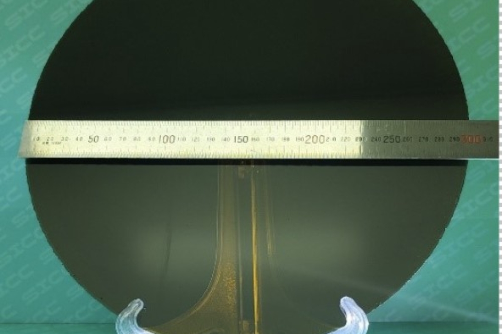
China has recently unveiled a groundbreaking manufacturing line for 300-mm silicon carbide substrates, marking a pivotal achievement in advanced semiconductor fabrication. Entirely conceptualized and executed with domestic innovations, this initiative signifies a leap forward in production scale and capability. The newly operational facility offers chipmakers substantially increased output per wafer and boasts significant cost-effectiveness gains, transforming components production for key technology sectors.
By expanding capacity with larger, high-purity silicon carbide substrates, manufacturers benefit from the ability to derive approximately two and a half times more chips from each wafer compared to smaller formats. Concurrently, the operational costs involved in fabrication see a notable decline, dropping by an estimated 40% relative to previous parameters. Such enhancements catalyze improved supply chain resilience and position the country to capture a larger slice of the global semiconductor manufacturing market.
Applications demanding these advanced substrates are diverse and rapidly growing. Sectors such as automotive electronics, telecommunications infrastructure, and renewable energy technologies are experiencing heightened material requirements driven by electric mobility, 5G network deployment, and solar energy integration. Consequently, this leap in manufacturing sophistication is expected to create ripple effects across these interrelated fields, spurring innovation and enabling more efficient and cost-effective device production.
The transition to larger substrate diameters represents a significant evolution in fabrication processes. The move from conventional dimensions to 300-mm formats allows for more chips per wafer, benefiting yield and throughput, which are vital parameters for keeping pace with global demand and industry competition. This scale-up also inherently reduces the per-unit production cost due to economies of scale and process optimization.
Achieving high material purity and minimized crystal defects in these wafers is equally critical. The indigenous development focuses heavily on mastering crystal growth techniques that control dislocation densities and eliminate microdefects, which are known to impact device reliability and performance. Such precision in substrate quality translates into more robust and efficient power electronics and microchips used in critical applications.
The enhanced production line thus enables the manufacture of substrates that serve in high-voltage and high-frequency devices. These are key components in electric vehicles’ powertrains, enhancing energy efficiency and driving range. Meanwhile, telecommunications equipment leveraging these substrates benefits from superior thermal management and signal integrity, fundamental for the expansion of next-generation wireless networks.
This development is expected to reshape competitive dynamics in the semiconductor supply chain. The increased domestic capacity for wafer fabrication reduces reliance on imports for critical materials, thus improving supply stability amid fluctuating international trade conditions. The ability to supply advanced substrates at competitive costs is likely to increase market capture, influencing regional technology leadership and trade balances.
The capacity to develop such sophisticated substrates fully within national borders also fosters a more self-sufficient ecosystem encompassing equipment, materials, and fabrication techniques. This integrated capability fortifies the manufacturing base against external disruptions and enhances collaboration between material producers and device manufacturers.
Moreover, the scalability achieved with large-diameter substrates empowers manufacturers to meet the growing requirements of various cutting-edge sectors. The automotive industry's switch to electrification and the ongoing roll-out of digital infrastructure initiatives require high-performance, reliable components that benefit directly from substrate improvements. Likewise, solar energy applications demand materials that enable efficient power conversion, a niche where the enhanced substrates play a pivotal role.
The significance of this new wafer production line extends beyond immediate manufacturing gains. By establishing a robust foundation for producing wide bandgap semiconductors, the industry can accelerate advancements in energy-efficient electronics and electromobility solutions. This progress lays the groundwork for more sophisticated power devices and communication modules that operate at elevated frequencies and voltages.
As demand intensifies in applications such as electric vehicle power electronics, 5G base stations, and photovoltaic systems, the ability to support these sectors reliably and competitively becomes a critical factor for technological leadership. With scaling up of indigenous production capabilities, the path is set for sustainable growth and integration of advanced materials into mainstream electronic systems worldwide.
In sum, elevating substrate size and purity through domestically sourced innovation reflects a strategic convergence of technology, manufacturing efficiency, and market responsiveness. This milestone is more than an incremental step; it signifies a pronounced shift in how materials critical to the semiconductor supply chain are produced, distributed, and optimized for future digital and energy applications.

.jpg)

